ANALOGUE ELECTRONICS I
| Site: | Hands On Learning |
| Course: | Hands On Learning |
| Book: | ANALOGUE ELECTRONICS I |
| Printed by: | |
| Date: | Wednesday, 2 July 2025, 3:06 AM |
1. The Semiconductor Diode
A diode is made from a small piece of semiconductor material, usually silicon, in which half is doped as a p region and half is doped as an n region with a pn junction and depletion region in between. The p region is called the anode and is connected to a conductive terminal. The n region is called the cathode and is connected to a second conductive terminal. The basic diode structure and schematic symbol are shown below.

The figure below shows typical diode packages for surface mounting on a printed circuit board.
1.1. Biasing
This is the process of connecting a DC voltage source across a diode so that the diode can conduct current in one direction and block it in the other direction.
Under no Bias conditions (i.e. bias voltage = 0 V), a diode doesn’t conduct current due to the barrier potential associated with the depletion region. That is, in the absence of an applied bias across a semiconductor diode, the net flow of charge in one direction is zero as shown below.

Diode can either be forward biased or reverse biased:
1.1.1 Forward Biasing (VBIAS > 0 V)
Forward bias is the condition that allows current through the pn junction. Figure 2–3 shows a dc voltage source connected by conductive material (contacts and wire) across a diode in the direction to produce forward bias. This external bias voltage is designated as VBIAS. The resistor limits the forward current to a value that will not damage the diode. Notice that the negative side of VBIAS is connected to the n region of the diode and the positive side is connected to the p region. This is one requirement for forward bias. A second requirement is that the bias voltage, VBIAS, must be greater than the barrier potential.


Because like charges repel, the negative side of the bias-voltage source “pushes” the free electrons, which are the majority carriers in the n region, toward the pn junction. This flow of free electrons is called electron current. The negative side of the source also provides a continuous flow of electrons through the external connection (conductor) and into the n region.
The bias-voltage source imparts sufficient energy to the free electrons for them to overcome the barrier potential of the depletion region and move on through into the p region.
Once in the p region, these conduction electrons have lost enough energy to immediately
combine with holes in the valence band.
Now, the electrons are in the valence band in the p region, simply because they have lost too much energy overcoming the barrier potential to remain in the conduction band. Since unlike charges attract, the positive side of the bias-voltage source attracts the valence electrons toward the left end of the p region. The holes in the p region provide the medium or “pathway” for these valence electrons to move through the p region. The valence electrons move from one hole to the next toward the left. The holes, which are the majority carriers in the p region, effectively (not actually) move to the right toward the junction. This effective flow of holes is the hole current.
As the electrons flow out of the p region through the external connection (conductor) and to the positive side of the bias-voltage source, they leave holes behind in the p region; at the same time, these electrons become conduction electrons in the metal conductor. Recall that the conduction band in a conductor overlaps the valence band so that it takes much less energy for an electron to be a free electron in a conductor than in a semiconductor and that metallic conductors do not have holes in their structure. There is a continuous availability of holes effectively moving toward the pn junction to combine with the continuous stream of electrons as they come across the junction into the p region.
When forward bias is applied, the free electrons are provided with enough energy from the bias-voltage source to overcome the barrier potential and effectively “climb the energy hill” and cross the depletion region. The energy that the electrons require in order to pass through the depletion region is equal to the barrier potential. In other words, the electrons give up an amount of energy equivalent to the barrier potential when they cross the depletion region. This energy loss results in a voltage drop across the pn junction equal to the barrier potential (0.7 V). An additional small voltage drop occurs across the p and n regions due to the internal resistance of the material. For doped semiconductor materials, this resistance, called the dynamic resistance, is very small and can usually be neglected.
1.1.1.1 The Effect of Forward Bias on the Depletion Region
The depletion region narrows and a voltage drop is produced across the pn junction when the diode is forward-biased. As more electrons flow into the depletion region, the number of positive ions is reduced. As more holes effectively flow into the depletion region on the other side of the pn junction, the number of negative ions is reduced. This reduction in positive and negative ions during forward bias causes the depletion region to narrow, as indicated in the figure below.


1.2. Shockley’s equation
2. TRANSISTOR CHARACTERISTICS AND BIASING
A transistor is a semiconductor device used to amplify or switch electronic signals and electrical power. It is composed of semiconductor material usually with at least three terminals for connection to an external circuit. A voltage or current applied to one pair of the transistor's terminals controls the current through another pair of terminals. Because the controlled (output) power can be higher than the controlling (input) power, a transistor can amplify a signal. Today, some transistors are packaged individually, but many more are found embedded in integrated circuits.
Transistor = Transfer + Resistor. Transistor is a device which transfers its resistance from high to low. Due to this property a transistor amplifies any input signal and transfers it to the output part of the amplifier. We can control the amplification by changing resistance values of transistors.
There are two basic types of transistors: the bipolar junction transistor (BJT) and the field-effect transistor (FET). The bipolar junction transistor is used in two broad areas of electronics: (1) as a linear amplifier to boost an electrical signal and (2) as an electronic switch.
2.1. Bipolar Junction Transistor
The bipolar junction transistor consists of two back-to-back P-N junctions manufactured in a single piece of a semiconductor crystal as shown in figure (a) below. That is, the BJT is constructed with three doped semiconductor regions separated by two pn junctions. These two junctions give rise to three regions called emitter, base and collector. Physical representations of the two types of BJTs are shown in Figures (b) and (c). One type consists of two n regions separated by a p region (npn), and the other type consists of two p regions separated by an n region (pnp). The term bipolar refers to the use of both holes and electrons as current carriers in the transistor structure.

The pn junction joining the base region and the emitter region is called the base-emitter junction. The pn junction joining the base region and the collector region is called the base-collector junction as shown.
The base region is lightly doped and very thin compared to the heavily doped emitter and the moderately doped collector regions. The emitter is heavily doped because its main function is to supply majority charge carries (either electrons or holes) to the base. The main function of the collector (as indicated by its name) is to collect majority charge carriers coming from the emitter and passing through the base. The standard schematic symbols for the npn and pnp bipolar junction transistors are shown below.

The arrowhead is always at the emitter (not at the collector) and in each case, its direction indicates the conventional direction of current flow. For a PNP transistor, arrowhead points from emitter to base meaning that emitter is positive with respect to base (and also with respect to collector) For NPN transistor, it points from base to emitter meaning that base (and collector as well) is positive with respect to the emitter. Note that in a transistor, for normal operation, the collector and base have the same polarity with respect to the emitter.
In most transistors, collector region is made physically larger than the emitter region because it has to dissipate much greater power. Because of this difference, there is no possibility of inverting the transistor i.e. making its collector the emitter and its emitter the collector.
1.1.1 Basic BJT Operation
In order for a BJT to operate properly as an amplifier, the two pn junctions must be correctly biased with external dc voltages.
1.1.1.1 Transistor Biasing
For proper working of a transistor, it is essential to apply voltages of correct polarity across its two junctions. It is worthwhile to remember that for normal operation; emitter-base junction is always forward biased and collector-base junction is always reverse- biased. This type of biasing is known as forward-reverse biasing (One p–n junction of a transistor is reverse-biased, whereas the other is forward-biased.).
In the figure below, two batteries respectively provide the dc emitter supply voltage VEE and collector supply voltage VCC for properly biasing the two junctions of the transistor.

or

NB: For a PNP transistor, both collector and base are negative with respect to the emitter (the letter N of Negative being the same as the middle letter of PNP). Of course, collector is more negative than base. Similarly, for NPN transistor, both collector and base are positive with respect to the emitter (the letter P of Positive being the same as the middle letter of NPN). Again, collector is more positive than the base. All these are shown below.

It may be noted that different potentials have been designated by double subscripts. The first subscript always represents the point or terminal which is more positive (or less negative) than the point or terminal represented by the second subscript. For example, in Fig (a) above, the potential difference between emitter and base is written as VEB (and not VBE) because the emitter is positive with respect to the base. Now, between the base and collector themselves, collector is more negative than base. Hence, their potential difference is written as VBC and not as VCB. Single subscripted voltages such as VB, VC, and VE are dc voltages from the transistor terminals to ground while IB, IC, and IE are the dc transistor currents. Similarly, single subscripted voltages such as Vb, Vc, and Ve are ac voltages from the transistor terminals to ground.
1.1.1.2 Transistor action
For a silicon p-n-p transistor, biased as shown in Figure 12.2(a) below, if the base-emitter junction is considered on its own, it is forward biased and a current flows. This is depicted in Figure 12.3(a). For example, if RE is 1000Ω, the battery is 4.5V and the voltage drop across the junction is taken as 0.7 V, the current flowing is given by (4.5 - 0.7) V /1000 Ω = 3.8 mA.


When the base-collector junction is considered on its own, as shown in Figure 12.3(b), it is reverse biased and the collector current is something less than 1 µA. However, when both external circuits are connected to the transistor, most of the 3.8 mA of current flowing in the emitter, which previously flowed from the base connection, now flows out through the collector connection due to transistor action.
In a p-n-p transistor, connected as shown in Figure 12.2(a), transistor action is accounted for as follows:
a). The majority carriers in the emitter p-type material are holes
b). The base-emitter junction is forward biased to the majority carriers and the holes cross the junction from the emitter region into the base region.
c). The base region is very thin and is only lightly doped with electrons so although some electron-hole pairs (electron-hole combinations) are formed, many holes are left in the base region
d). The base-collector junction is reverse biased to electrons in the base region and holes in the collector region, but forward biased to holes in the base region; these holes are attracted by the negative potential at the collector terminal.
e). A large proportion of the holes in the base region cross the base-collector junction into the collector region, creating a collector current; conventional current flow is in the direction of hole movement.
The transistor action is shown diagrammatically below. For transistors having very thin base regions, up to 99.5% of the holes leaving the emitter cross the base collector junction.

In an n-p-n transistor, connected as shown in Figure 12.2(b), transistor action is accounted for as follows:
a). The majority carriers in the n-type emitter material are electrons.
b). The base-emitter junction is forward biased to these majority carriers and electrons cross the junction and appear in the base region.
c). The base-emitter junction is forward biased to these majority carriers and electrons cross the junction and appear in the base region.
d). The base-collector junction is reverse biased to holes in the base region and electrons in the collector region, but is forward biased to electrons in the base region; these electrons are attracted by the positive potential at the collector terminal.
e). A large proportion of the electrons in the base region cross the base collector junction into the collector region, creating a collector current.
The transistor action is shown diagrammatically in Figure 12.5. Conventional current flow is taken to be in the direction of hole flow, that is, in the opposite direction to electron flow, hence the directions of the conventional current flow are as shown in Figure 12.5.

For a p-n-p transistor, the base-collector junction is reverse biased for majority carriers. However, a small leakage current, ICBO flows from the base to the collector due to thermally generated minority carriers (electrons in the collector and holes in the base), being present. The base-collector junction is forward biased to these minority carriers. If a proportion, α, (having a value of up to 0.995 in modern transistors), of the holes passing into the base from the emitter, pass through the base-collector junction, then the various currents flowing in a p-n-p transistor are as shown in Figure 12.6(a).

Similarly, for an n-p-n transistor, the base-collector junction is reversed biased for majority carriers, but a small leakage current, ICBO flows from the collector to the base due to thermally generated minority carriers (holes in the collector and electrons in the base), being present. The base-collector junction is forward biased to these minority carriers. If a proportion, α, of the electrons passing through the base-emitter junction also pass through the base-collector junction then the currents flowing in an n-p-n transistor are as shown in Figure 12.6(b).
For the transistor as depicted in Figure 12.4, the emitter is relatively heavily doped with acceptor atoms (holes). When the emitter terminal is made sufficiently positive with respect to the base, the base-emitter junction is forward biased to the majority carriers. The majority carriers are holes in the emitter and these drift from the emitter to the base. The base region is relatively lightly doped with donor atoms (electrons) and although some electron-hole recombination’s take place, perhaps 0.5%, most of the holes entering the base, do not combine with electrons.
The base-collector junction is reverse biased to electrons in the base region, but forward biased to holes in the base region. Since the base is very thin and now is packed with holes, these holes pass the base-emitter junction towards the negative potential of the collector terminal. The control of current from emitter to collector is largely independent of the collector-base voltage and almost wholly governed by the emitter-base voltage. The essence of transistor action is this current control by means of the base-emitter voltage.
In a p-n-p transistor, holes in the emitter and collector regions are majority carriers, but are minority carriers in the base region. Also thermally generated electrons in the emitter and collector regions are minority carriers as are holes the base region. However, both majority and minority carriers contribute towards the total current flow (see Figure 12.6(a)). It is because a transistor makes use of both types of charge carriers (holes and electrons) that they are called bipolar. The transistor also comprises two p-n junctions and for this reason it is a junction transistor. Hence the name - bipolar junction transistor.
1.1.1.3 Transistor Currents
Consider the figures shown below:

Applying Kirchhoff's Current Law to the above figures, we have
![]()
In general, a small part (about 1 - 2%) of emitter current goes to supply base current and the remaining major part (98 - 99%) goes to supply collector current. This statement is true regardless of transistor type or transistor configuration.

1.1.2 Transistor Circuit Configurations
There are three types of circuit connections (called configurations) for operating a transistor:
a) Common-base (CB).
b) Common-emitter (CE).
c) Common-collector (CC).
The term ‘common’ is used to denote the electrode that is common to the input and output circuits. Because the common electrode is generally grounded, these modes of operation are frequently referred to as grounded-base, grounded-emitter and grounded-collector configurations as shown below for a PNP – transistor. Since a transistor is a 3-terminal (and not a 4-terminal) device, one of its terminals has to be common to the input and output circuits.

1.1.2.1 CB Configuration
In this configuration, emitter current IE is the input current and collector current IC is the output current. The input signal is applied between the emitter and base whereas output is taken out from the collector and base as shown below (for n-p-n transistor):

Static characteristics for a common-base circuit
Static characteristics are curves which represent relationships between different d.c. currents and voltages of a transistor. They are helpful in studying the operation of a transistor when connected in a circuit.
(i) Input characteristic.
The figure below shows an arrangement for determining the static characteristics of an n–p–n transistor used in a common-base circuit.

OR

The input characteristic can be obtained by varying R1, which varies VEB, and noting the corresponding values of IE. This is repeated for various values of VCB. It will be found that the input characteristic is almost independent of VCB and it is usual to give only one characteristic as below.
The input to a common-base transistor is the emitter current, IE, and can be varied by altering the base emitter voltage VEB. The base-emitter junction is essentially a forward biased junction diode, so as VEB is varied, the current flowing is similar to that for a junction diode, as shown below for a silicon transistor.


The figure above is called the input characteristic for an n-p-n transistor having common-base configuration. The variation of the collector-base voltage VCB has little effect on the characteristic. A similar characteristic can be obtained for a p-n-p transistor, these having reversed polarities.
(ii) Output characteristics.
The value of the collector current IC is very largely determined by the emitter current, IE. IE is set to a suitable value by adjusting R1. For various values of VCB, set by adjusting R2, IC is noted. This procedure is repeated for various values of IE. To obtain the full characteristics, the polarity of battery V2 has to be reversed to reduce IC to zero. This must be done very carefully or else values of IC will rapidly increase in the reverse direction and burn out the transistor.
For a given value of IE the collector-base voltage, VCB, can be varied and has little effect on the value of IC. If VCB is made slightly negative, the collector no longer attracts the majority carriers leaving the emitter and IC falls rapidly to zero. That is, IE is kept constant while VCB is varied and IC is observed. The test is repeated for various values of the emitter current and the results are plotted as below:

2.2. Field-Effect Transistors (FETs)
The field-effect transistor (FET) is a transistor that uses an electric field to control the electrical behaviour of the device. It is a three-terminal device used for a variety of applications that match, to a large extent, those of the BJT transistor. Although there are important differences between the two types of devices, there are also many similarities. The primary difference between the two types of transistors is the fact that: a BJT is a current-controlled device; that is, the base current controls the amount of collector current. A FET is a voltage-controlled device, where the voltage between two of the terminals (gate and source) controls the current through the device.
FETs are unipolar devices because, unlike BJTs that use both electron and hole current, they operate only with one type of charge carrier. The two main types of FETs are the junction field-effect transistor (JFET) and the metal oxide semiconductor field-effect transistor (MOSFET). The term field-effect relates to the depletion region formed in the channel of a FET as a result of a voltage applied on one of its terminals (gate).
3. LARGE SIGNAL (POWER) AMPLIFIERS
An amplifier receives a signal from an input source and provides a larger version of the signal to some output device or to another amplifier stage. An input signal is generally small (a few millivolts from a cassette or CD input, or a few microvolts from an antenna) and needs to be amplified sufficiently to operate an output device (speaker or other power-handling device). In small-signal amplifiers, the main factors are usually amplification linearity and magnitude of gain. Since signal voltage and current are small in a small-signal amplifier, the amount of power-handling capacity and power efficiency are of little concern. A voltage amplifier provides voltage amplification primarily to increase the voltage of the input signal. Large-signal or power amplifiers, on the other hand, primarily provide sufficient power to an output load to drive a speaker or other power device, typically a few watts to tens of watts. The main features of a large-signal amplifier are the circuit’s power efficiency, the maximum amount of power that the circuit is capable of handling, and the impedance matching to the output device.
NB: Power amplifiers are those amplifiers that have the objective of delivering power to a load. This means that components must be considered in terms of their ability to dissipate heat.
One method used to categorize amplifiers is by class. Basically, amplifier classes represent the amount the output signal varies over one cycle of operation for a full cycle of input signal. They are:
i). Class A
ii). Class B
iii). Class AB
iv). Class C
v). Class D
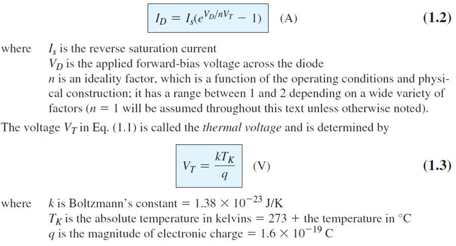
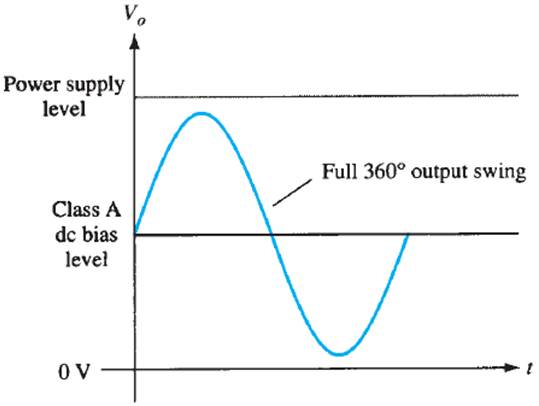
3.1. The Class A Power Amplifier
The output signal varies for a full 360° of the input signal. The figure below shows that this requires the Q - point to be biased at a level so that at least half the signal swing of the output may vary up and down without going to a high enough voltage to be limited by the supply voltage level or too low to approach the lower supply level, or 0 V in this description. This means that the amplifier is biased such that it always operates in the linear region (active region) where the output signal is an amplified replica of the input signal.
In a small-signal amplifier, the ac signal moves over a small percentage of the total ac load line. When the output signal is larger and approaches the limits of the ac load line, the amplifier is a large-signal type. Both large-signal and small-signal amplifiers are considered to be class A if they operate in the linear region at all times, as illustrated below.
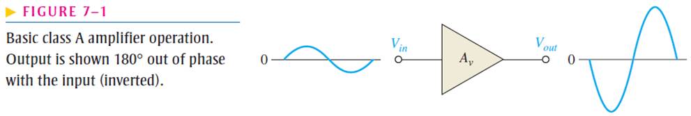
3.2. The Class B Amplifiers
A class B circuit provides an output signal varying over one-half the input signal cycle, or for 1800 of signal. That is, an amplifier is biased at cutoff so that it operates in the linear region for 1800 of the input cycle and is in cutoff for 1800. This is illustrated below:
Obviously, the output is not a faithful reproduction of the input if only one half-cycle is present. Two class B operations—one to provide output on the positive-output half-cycle and another to provide operation on the negative-output half-cycle—are necessary. The combined half-cycles then provide an output for a full 360° of operation. This type of connection is referred to as push–pull operation. Note that class B operation by itself creates a very distorted output signal since reproduction of the input takes place for only 180° of the output signal swing.